Get A Quote

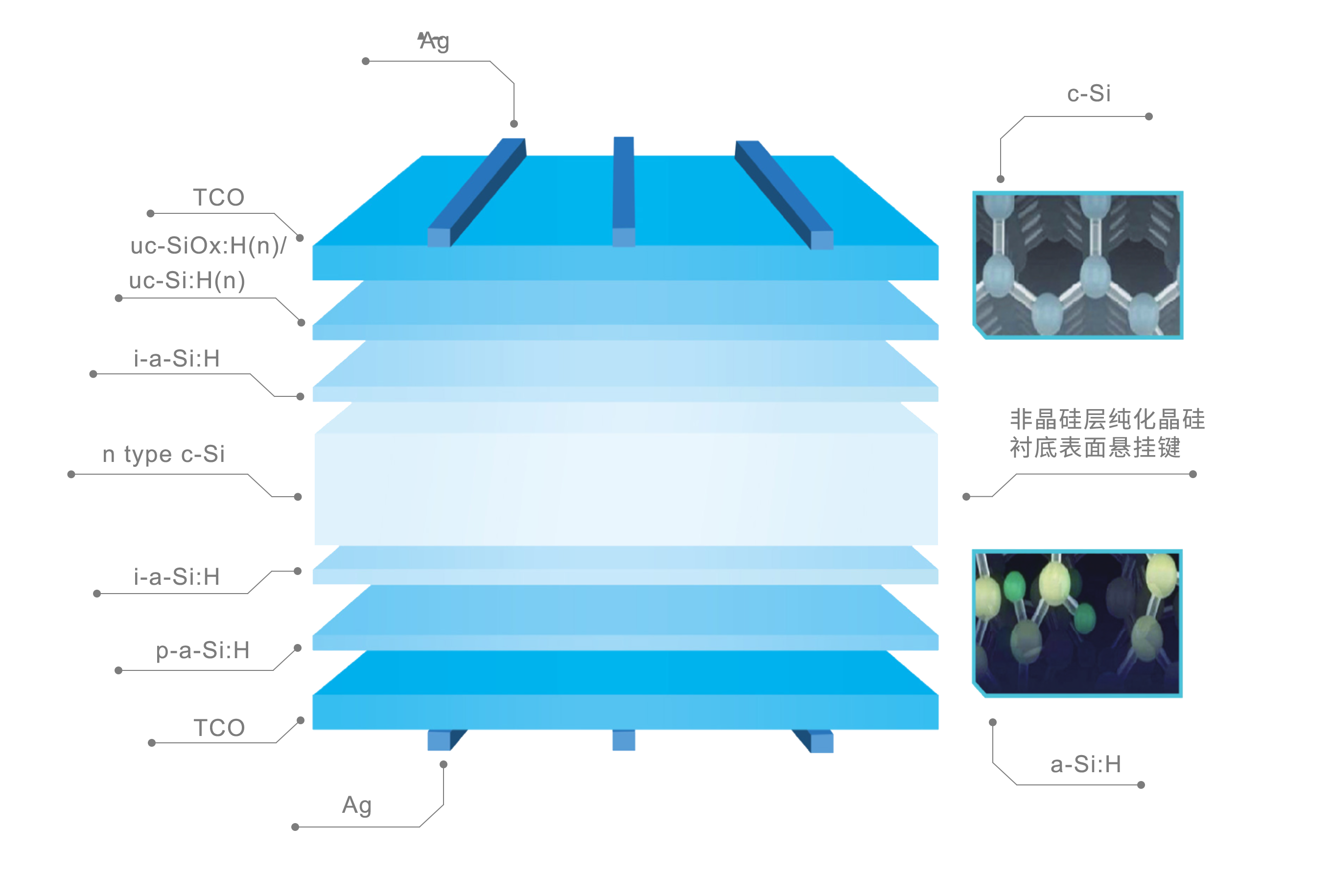
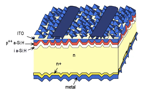
Heterojunction technology (HJT) is a N-type bifacial solar cell technology, by leveraging N-type monocrystalline silicon as a substratum and depositing silicon-based thin films with different characteristics and transparent conductive films on the front and rear surfaces respectively.
Combining with the benefits of crystalline silicon and amorphous silicon thin-fim technologies, HJT technology has excellent photoabsorption and passivation effects, as well as outstanding efficiency and performance. HJT panels are one of the technologies to improve the conversion rate and power output to the highest level, also represent the trend of the new generation of solar cell platform technology.
Heterojunction (HJT) solar cell technology, as a platform technology, can be combined with thin film solar technology and perovskite solar technology, with a maximum photoelectric conversion efficiency of over 30%. Solar power generation is a disruptive technology that will gradually replace existing technologies such as PERC and TOPCon in the next 3-5 years, becoming the mainstream technology direction of solar power generation.
According to optimistic predictions from third-party organizations, the shipment volume of HJT modules will rapidly increase from 15GW to 643GW from 2023 to 2027, and its market share in photovoltaic module shipments will significantly increase from 4.3% up to 90%.
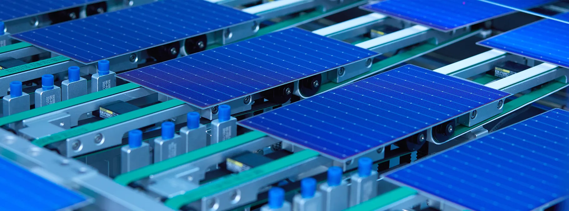
HJT's core process flow only has 4 steps. The shorter process flow can help improve the yield rate and reduce costs such as labor and operation and maintenance.
High bifacial ratio: HJT battery has a bifacial symmetrical structure, and the bifacial ratio can reach up to 95%. Low temperature coefficient: The temperature coefficient of HJT is -0.24%/℃, which is lower than PERC (-0.35%/℃) and (TOPCon-0.30%/℃). Low attenuation rate: HJT has no PID and LID effects, and will last for 30 years. In a long life cycle, HJT generates higher power.
The double-sided symmetrical structure of HJT reduces the mechanical stress of the silicon wafer and improves the overall wafer yield during the preparation process. The low-temperature process also reduces the possibility of warping of the silicon wafer when heated, which is more conducive to thinning.
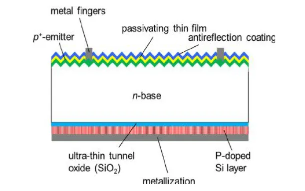
The entire process of HJT is made in an environment below 200°C. In contrast, the temperature of the phosphorus expansion part of PERC needs to be higher than 850°C, and the temperature of the boron expansion part of TOPCon is above 1100°C. The low-temperature process helps reduce thermal damage during silicon wafer preparation and saves fuel.
HJT cells mainly absorb infrared light, while perovskite cells have a high utilization rate of light waves from short wavelengths to visible light wavelengths. The stacking of the two completes the "eclectic" absorption spectrum and can open up the ceiling of theoretical conversion efficiency.
Higher conversion efficiency, ultra-thin applications, and low-temperature manufacturing processes help reduce the carbon emissions of a single silicon wafer.
Laboratory maximum efficiency:24.06%
The pass rate exceeds:>98%
The double-sided rate:~70%
Temperature coefficient:-0.34%
Cell peak process temperature:~800℃
Celsius cell manufacturing process number:8
Silicon wafer thickness:150μm
Cell silver paste usage:9.6mg/W
Carbon footprint data:550gCO2/W
Laboratory maximum efficiency:26.7%
The pass rate exceeds:>97%
The double-sided rate:~85%
Temperature coefficient:-0.30%
Cell peak process temperature:~1000℃
Celsius cell manufacturing process number:11
Silicon wafer thickness:130μm
Cell silver paste usage:12.1mg/W
Carbon footprint data:480gCO2/W
Laboratory maximum efficiency:27.08%
The pass rate exceeds:>98%
The double-sided rate:≥95%
Temperature coefficient:-0.24%
Cell peak process temperature:~200℃
Celsius cell manufacturing process number:4
Silicon wafer thickness:<100μm
Cell silver paste usage:<10mg/W
Carbon footprint data:<400gCO2/W
Please read on, stay posted, subscribe, and we welcome you to tell us what you think.